CNT transistors using single-walled carbon nanotubes (CNTs) as a semiconductor material have finally ushered in a period of accelerated development, and there has been an attempt to integrate CNT transistors on chips as an initial computer trial system. Subhaish Mitra, an assistant professor of electrical engineering and computer science at Stanford University in the United States, produced a CNT microprocessor that integrates 178 CNT transistors (Figure 1). Upon confirmation, the processor can operate as a programmable computer through an external memory. This CNT computer follows the basic structure of the current von Neumann computer. The operating frequency is 1 kHz, which is equivalent to the primary computer using transistors in the early 1950s (Note 1). (Note 1) The reason is that the operating frequency is low and the electrode used for operation verification is large. It is not a limitation of the CNT transistor itself. The arithmetic circuit that performs AND and XOR uses 20 CNT transistors, and the D latch circuit that temporarily stores data uses 9 CNT transistors. The computing content is programmable, and it can execute 20 basic instructions in the MIPS architecture directive set by Imagination Technologies (formerly MIPS Technology, UK) (Note 2). In addition to this, it is also possible to run a self-contained OS that can perform multitasking. (Note 2) The 20 instructions are: AND, ANDI, BGEZ, BLEZ, BLTZ, BNE, J, LB, NOOP, OR, ORI, SB, SLL, SLLV, SRA, SRL, SRLV, SUBU, XOR, XORI. Shoulder 1950s computer Stanford University's SEM image of the CNT microprocessor. It consists of 178 CNT transistors and measures about 7mm x 0.8mm. The arithmetic operation uses 20 CNT transistors. (Photo: Stanford University) Use large currents to destroy metallic CNTs This kind of computer's CNT transistor uses a CNT that points to a uniform channel layer (Figure 2). The CNTs were first grown on a crystal substrate and then transferred to a Si/SiO2 substrate using a thermal release tape. In CNT, the proportion of semiconductor type accounts for more than 99.99%. CNT transistor configuration (a) and manufacturing process (b). At the wafer level, large currents are used to destroy metallic CNTs and the purity of semiconductor CNTs is raised to 99.99% or more. In general, the ratio of the semiconductor type to the metal type is 2 to 1 in single-walled CNTs, which is the biggest issue for the development of CNT transistors. Since the metal-type CNTs doped in the semiconductor-type CNTs cause a short circuit between the electrodes, the transistors will not be able to perform as expected. This time, Mitra et al. eliminated most of the metallic CNTs of each integrated circuit one by one in the latter half of the manufacturing process, and solved the problem by this method. The name of the method is called VMR (VLSI-compatible metallic CNT removal). Specifically, CNT transistors are first fabricated on Si/SiO2 wafers, gold (Au) temporary wirings are made, large currents are passed through the circuit, and metal-type CNTs are destroyed. Then, the Au wiring is removed, and formal wiring is performed using metals such as platinum (Pt). "The VMR can be used regardless of the size of the circuit" (Mitra). Catching up with the computer in the 1970s On the other hand, CNT transistors fabricated using a coating process also have precedents that operate at frequencies above 500 kHz. If this transistor is used to make a CNT computer, the operating frequency will reach the level of the first microprocessor "4004" and "8008" that Intel announced in the early 1970s. This coating type CNT transistor is jointly developed by NEC, the Technical Research Alliance Single Layer CNT Fusion Material Research and Development Agency (TASC), and the University of Tokyo. "The work performance is sufficient for the line control circuit of a flexible display and sensing film" (NEC). NEC stated that there are two major improvements. One is the formation of electrodes using the "Super Inkjet (SIJ) method*", which greatly reduced the electrode width from about 50 μm in the past to 2 μm (FIG. 3). This reduces gate overlap with source/drain and reduces parasitic capacitance to 1/10. The operating frequency has thus been greatly improved. * Superjet (SIJ) = inkjet technology or device with a droplet volume of only 1f (fly) L. Developed by the Japan Institute of Industrial Technology in 2005. Coating type CNT transistor (a) produced by trial by NEC et al., Superjet ink (SIJ) apparatus (b) used for coating, and effect of reducing parasitic capacitance (c). Because of the small parasitic capacitance, the operating frequency is as high as 500 kHz or more. (Figures: (a), (c) are produced by Nikkei Electronics based on NEC data) Semiconductor CNTs have a purity of more than 98% Another improvement is to greatly improve the accuracy of the technique of separating the metal and semiconductor CNTs in solution using electrophoresis. The method previously used by NEC can increase the purity of semiconducting CNTs to 95% or more. However, the CNT dispersion stabilizer used in this method will become an impurity residue, and the progress in improving the transistor performance will not be as expected. This time, by increasing the purity of semiconductor CNTs to 98% or more, the residual amount of dispersion stabilizers has been reduced to 1/50 of the past. The quality of the transistor's semiconductor layer has been greatly improved. In terms of output current, the original -0.6μA current has increased to -6.2μA, which is 10 times that of the past. (Reporter: Nozawa Tetsuru, Nikkei Electronics) Auto Led Headlight,Led Headlights For Cars,Led Headlamp For Car,Automotive Led Headlights CHANGZHOU CLD AUTO ELECTRICAL CO.,LTD , https://www.cld-leds.com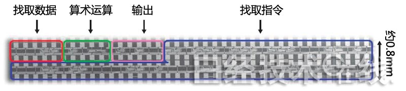
Figure 1: One hundred and seventy-nine CNT transistors form a CNT microprocessor 
Figure 2: Use of large currents to destroy metal-type CNTs after IC formation 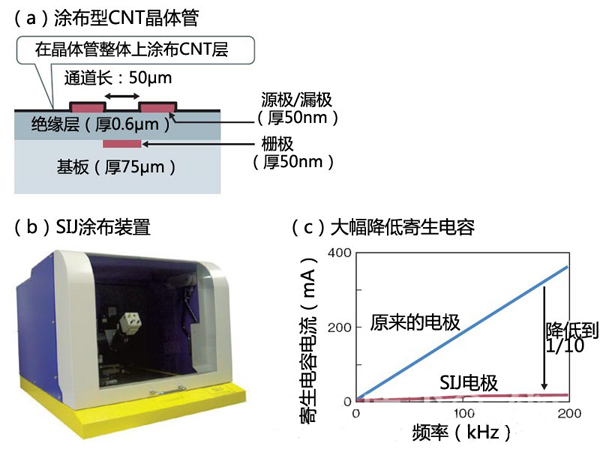
Figure 3: Using printing technology to achieve operating frequencies above 500kHz